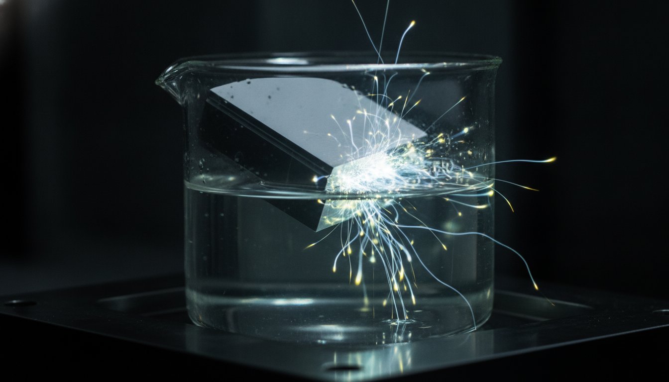
The assumption that high dielectric strength must inherently compromise thermal conductivity is a legacy constraint that modern material science has finally dismantled. For engineers working in the semiconductor and aerospace sectors, the dielectric properties of PEO coatings represent a strategically tunable variable rather than a fixed material limitation. You’re likely familiar with the high stakes of dielectric breakdown in high-vacuum environments or the thermal dissipation issues that plague traditional insulators. These challenges often stem from non-uniform coating thickness, which can lead to premature electrical failure in critical components where precision is paramount.
We understand that in high-precision manufacturing, failure isn’t an option. This guide provides a technical roadmap to mastering breakdown voltage and dielectric strength through precise bipolar pulse control and optimized electrolyte chemistry. You’ll discover how to leverage next-gen Plasma Electrolytic Oxidation to achieve high dielectric strength without sacrificing thermal performance. We’ll examine how precision-engineered coatings can reduce plasma non-uniformity in etch chambers and identify the specific power configurations needed to future-proof your high-performance electronic components. From reducing energy consumption with low-voltage processes to achieving adhesion strengths of 70 MPa, we’ll explore the strategic shifts necessary for industrial excellence.
Key Takeaways
- Learn how to engineer the dielectric properties of PEO coatings by manipulating process parameters to achieve superior breakdown voltage in high-vacuum semiconductor environments.
- Discover the critical role of phase composition and porosity management in eliminating electrical failure points or discharge channels within the ceramic layer.
- Compare the technical performance of PEO against traditional treatments such as Hard Anodizing and PVD to identify the most resilient solution for high-stakes electronic applications.
- Identify strategic methods to reduce plasma non-uniformity in etch chambers through precise control of coating thickness and dielectric stability.
- Explore how the shift to Bipolar PEO technology enables the tuning of the “soft sparking” regime for next-generation insulation and thermal dissipation.
Understanding the Fundamentals of Dielectric Properties in PEO Coatings
Engineering high-performance electronic components requires more than surface-level insulation; it demands a deep understanding of material behavior under electrical stress. The dielectric properties of PEO coatings are defined by their ability to resist electrical conduction while supporting an electrostatic field. Unlike traditional polymer coatings that often degrade under extreme thermal loads, PEO layers are inherently ceramic. This crystalline structure provides a robust barrier against electrical failure in high-voltage and high-frequency applications. The ceramic nature of the coating ensures that insulation remains stable even as operating temperatures fluctuate, a critical factor for semiconductor chamber components.
Permittivity, or the dielectric constant, plays a strategic role in how these coatings manage energy storage and signal integrity. In high-frequency applications, a stable dielectric constant is necessary to prevent signal distortion and energy loss. By controlling the Plasma electrolytic oxidation (PEO) process parameters, engineers can tailor the density and phase composition of the oxide layer. This level of precision allows for the integration of coatings into complex optoelectronic systems where electrical impedance must be tightly managed.
To better understand the functional role of these coatings in industrial applications, watch this technical overview:
Dielectric Strength vs. Breakdown Voltage
It’s vital to distinguish between dielectric strength and breakdown voltage. Dielectric strength is an intrinsic material property, representing the maximum electric field a material can withstand without failing. For PEO, dielectric strength typically ranges from 10 to 50 V/µm. Breakdown voltage, conversely, is the actual voltage threshold where a specific component’s insulation fails. While increasing coating thickness generally raises the breakdown voltage, the relationship isn’t always linear. Defects or non-uniformities can create localized paths for current. Environmental factors like high humidity can lower effective performance, while high-vacuum environments demand extreme dielectric stability to prevent arcing.
The Physics of Plasma-Induced Insulation
The insulation provided by PEO is born from high-energy plasma reactions. During the process, localized micro-discharges convert the metal surface into a dense, non-conductive ceramic matrix. The growth begins with a thin, dense barrier layer, followed by a more complex porous functional layer. This mechanism is effectively “self-healing” during fabrication. If a discharge occurs at a weak point, the resulting plasma reaction immediately deposits new ceramic material to reinforce that area. This results in an integrated non-conductive matrix that outperforms traditional anodized layers in both durability and electrical resistance. For more detailed technical insights into process control, you can explore our latest research on the Bipolar PEO blog.
The Microstructural Engine: How Process Parameters Shape Dielectric Performance
The performance of a ceramic layer isn’t just a byproduct of the process; it’s the result of deliberate microstructural engineering. To optimize the dielectric properties of PEO coatings, engineers must look beyond surface thickness and focus on the internal architecture of the oxide matrix. The microstructure acts as the primary engine for electrical insulation, where phase composition and pore distribution determine whether a component survives or fails under high-voltage stress. Precision-engineered bipolar pulse control allows us to manipulate these variables with surgical accuracy, transforming a standard surface into a high-performance dielectric barrier.
Surface roughness also plays a secondary but critical role in electrical integrity. High peaks on a rough surface act as field concentrators, which can trigger localized breakdown even if the bulk material is sound. Achieving a dense, smooth finish is essential for components in high-vacuum environments where electrical arcing is a constant risk. If you’re looking to optimize these parameters for your specific alloy, exploring our PEO technology license solutions can provide the strategic framework needed for industrial-scale success.
Phase Engineering for Maximum Insulation
The ratio of alpha-alumina to gamma-alumina is the most significant factor in dielectric performance. Alpha-Al2O3 is essentially the “holy grail” for these applications because its crystalline structure offers superior hardness and significantly lower leakage current compared to its gamma counterpart. Driving this thermal transformation requires the intense, localized heat found in micro-discharges. By utilizing bipolar power units, we can tune the “soft sparking” regime to encourage alpha-phase growth without inducing the thermal cracking that often accompanies high-voltage DC processes. Recent innovations in PEO coatings suggest that this crystallinity is the primary defense against dielectric failure, with hardness levels reaching up to 2000 HV in well-optimized layers.
Anion Concentration and Growth Mechanisms
Electrolyte chemistry dictates the density and compactness of the growing layer. Research indicates that maintaining pH levels between 12.5 and 12.75 is optimal for balancing layer growth with surface quality. When aluminate and silicate concentrations are precision-matched, they create a synergistic effect that minimizes “discharge channels.” These channels are the primary pathways for electrical breakdown. If the alkalinity is too high, the process enters a “dissolution dominant” regime where the coating dissolves as quickly as it forms. This results in a porous, unstable layer that compromises the dielectric properties of PEO coatings. Strategic management of these anion concentrations ensures a dense, integrated matrix that serves as a reliable insulator for next-gen semiconductor chambers.
Comparative Analysis: PEO vs. Traditional Dielectric Surface Treatments
Selecting the right insulation strategy requires a rigorous evaluation of how different surface treatments perform under industrial stress. While Hard Anodizing and Physical Vapor Deposition (PVD) have served as industry standards for decades, they often fall short in high-stakes environments. The dielectric properties of PEO coatings provide a superior alternative because the layer is grown directly from the substrate metal. This creates an integrated chemical bond that resists delamination, a common failure point for sprayed or deposited coatings that rely on mechanical adhesion.
A critical advantage of the PEO process is its inherent ability to provide uniform coverage on complex geometries. Traditional treatments often suffer from the “edge effect,” where coating thickness tapers off at sharp corners, leading to localized electrical failure. Because the plasma discharge in PEO naturally migrates to areas of lower electrical resistance, it ensures consistent thickness across the entire component. This self-regulating mechanism is vital for precision-engineered robotics and aerospace components where geometric complexity is high.
PEO vs. Traditional Anodizing
Hard Anodizing (Type III) relies on a columnar pore structure that’s susceptible to moisture ingress. In humid environments, these pores can act as conductive pathways, significantly reducing the insulation capacity of the part. In contrast, PEO produces a more complex, interlocking ceramic matrix that effectively seals off these pathways. Thermal stability is another defining factor. While anodized layers may craze or crack at temperatures above 100°C, PEO coatings remain stable at much higher operating temperatures. This makes PEO the strategic choice for components that must maintain high dielectric strength during intense thermal cycling.
Ceramic Coating Performance Matrix
PEO stands as the definitive solution for high-voltage insulation due to its superior phase crystallinity and integrated bond strength.
- Adhesion Strength: PEO achieves up to 70 MPa, far exceeding the mechanical bond of PVD or thermal sprays.
- Hardness: Reaches up to 2000 HV, providing unmatched wear resistance alongside electrical insulation.
- Substrate Versatility: High dielectric constants are achievable across lightweight alloys, including aluminum, magnesium, and titanium.
- Weight Efficiency: High breakdown voltages are achieved with thinner layers, reducing the overall mass of aerospace and robotic assemblies.
When evaluating the cost-to-performance ratio, PEO offers long-term value by extending component life and reducing the risk of catastrophic electrical failure. For organizations looking to integrate these advantages into their production lines, our technical resources offer deeper insights into alloy-specific performance metrics.

Strategic Selection: Optimizing Dielectrics for Semiconductors and Optoelectronics
In the high-precision world of semiconductor fabrication, the dielectric properties of PEO coatings serve as a critical defense against plasma erosion and electrical instability. Etch chambers operate in high-power RF environments where even minor dielectric non-uniformity can trigger catastrophic arcing. By engineering the ceramic matrix to provide consistent insulation across all chamber surfaces, manufacturers can significantly reduce plasma non-uniformity. This level of control is vital for maintaining the integrity of the etching process and ensuring high-yield wafer production in next-gen facilities.
High-vacuum environments introduce additional complexities, particularly regarding outgassing and dielectric stability. Traditional insulators often release volatile compounds that contaminate sensitive semiconductor processes. PEO-grown ceramics are inherently stable and exhibit near-zero outgassing rates, making them the strategic choice for next-gen vacuum chambers. This stability ensures that the dielectric strength remains constant, preventing electrical failure during long-duration vacuum cycles where maintenance access is limited.
For Co-Packaged Optics (CPO) and high-density electronic housings, the challenge is balancing dielectric strength with efficient heat distribution. Magnesium alloys like AZ91D and AZ31 are increasingly used for their lightweight properties, yet they require specialized surface treatments to function as reliable insulators. PEO creates a precision-engineered ceramic layer on these alloys that facilitates rapid thermal dissipation while maintaining unmatched electrical resistance. This synergy is essential for preventing thermal throttling in high-speed data centers and robotic sensor arrays where space is at a premium.
Semiconductor Chamber Coating Excellence
Achieving dielectric uniformity is the primary objective when designing coatings for high-power RF environments. A non-uniform layer creates localized impedance variations, which are the leading cause of arcing in plasma etch chambers. High-purity ceramic layers are equally important because any metallic impurities within the coating can lead to wafer contamination. By integrating PEO into semiconductor equipment surface engineering strategies, companies can achieve the chemical purity and electrical consistency required for sub-7nm node production.
Optoelectronics and Lidar Applications
Lidar optical systems and high-density optoelectronic arrays demand surfaces that provide low electrical interference and superior thermal management. In robotic sensors, the strategic hardening of lightweight metals through PEO ensures that components withstand physical wear without losing their dielectric integrity. These coatings act as a thermal bridge, allowing heat to flow away from sensitive laser diodes while providing a robust electrical barrier. This dual-functionality is a cornerstone of future-proofing autonomous systems against environmental and electrical stress.
Explore how our Semiconductor Chamber Coating solutions can optimize your next-gen manufacturing process and enhance component reliability.
Future-Proofing Dielectric Performance with Bipolar PEO Technology
The transition from conventional DC power to bipolar pulse technology represents a fundamental shift in how we manage the dielectric properties of PEO coatings. Early PEO processes relied on high-voltage DC that often resulted in thermal cracking and coarse microstructures due to uncontrolled arc discharges. Bipolar power units offer a sophisticated alternative by allowing for the precise modulation of positive and negative pulses. This control effectively neutralizes the charge buildup that otherwise leads to destructive “hard” sparking. It’s this level of electrical precision that’s essential for scaling PEO from laboratory-scale prototypes to high-volume industrial production lines in the defense and aerospace sectors.
For industrial drones and aerospace systems, the weight-to-insulation ratio is a primary design constraint. Bipolar PEO technology allows for the creation of thinner, more resilient ceramic layers that provide the necessary insulation for high-power propulsion and electronic warfare systems. Transitioning from laboratory specifications to industrial-scale PEO processing requires a deep understanding of how power density affects the final dielectric properties of PEO coatings on large, complex components. By optimizing the pulse profile, we can ensure that every square millimeter of a component meets the rigorous standards required for next-gen performance.
The Role of Bipolar Power Units
Precision-engineered pulse shapes are the key to minimizing coating defects and achieving unmatched dielectric strength. By adjusting the duty cycle and frequency, engineers can drive the “soft sparking” regime, which favors the formation of dense, crystalline phases like alpha-alumina. This approach significantly reduces thermal stress during the oxidation process, preventing the micro-cracks that often compromise electrical integrity. Learn more about our PEO Bipolar Power Units for advanced material treatment and discover how digital control is revolutionizing surface science. These units don’t just provide power; they provide the strategic control necessary for future-proofing critical components.
Strategic Technology Licensing
Integrating advanced dielectric PEO capabilities into existing production lines doesn’t require a complete overhaul of your manufacturing infrastructure. Through strategic technology licensing, organizations can adopt integrated solutions that bridge the gap between laboratory R&D and industrial excellence. This roadmap ensures that next-gen aerospace and semiconductor components are equipped with the most resilient dielectric barriers available. The future of dielectric coatings is a software-defined hardware process where the pulse profile dictates the material’s performance. By leveraging these strategic partnerships, manufacturers can unlock the full potential of lightweight metals while maintaining the highest standards of reliability and innovation.
Advancing Industrial Excellence through Precision Dielectric Engineering
Mastering the dielectric properties of PEO coatings isn’t just about surface protection; it’s about unlocking the next generation of high-stakes industrial applications. We’ve explored how the shift from traditional anodizing to precision-engineered ceramic matrices enables superior breakdown voltage and thermal stability. By leveraging proprietary Bipolar PEO Power Unit technology, engineers can now tune the “soft sparking” regime to achieve dense crystalline structures that resist electrical failure in the most demanding environments. This level of control is essential for scaling laboratory successes into industrial-scale realities.
Whether you’re optimizing semiconductor chamber coatings for sub-7nm production or implementing advanced MAO solutions for AZ91D and AZ31 magnesium alloys, the strategic control of phase composition remains the definitive factor in component reliability. Our specialized expertise ensures that your integrated solutions are built for durability and innovation. We’re ready to help you navigate these complex material challenges with confidence and precision. It’s time to move beyond legacy constraints and embrace the potential of software-defined surface engineering.
Consult with our R&D team on your specific dielectric requirements today to ensure your high-performance components are future-proofed against electrical and thermal stress. Let’s build the future of material science together.
Frequently Asked Questions
What is the typical dielectric strength of a PEO coating on aluminum?
The typical dielectric strength of a PEO coating on aluminum ranges between 10 and 50 V/µm. This specific value is influenced by the phase composition of the layer, specifically the concentration of crystalline alpha-alumina. While thickness plays a role in the total breakdown voltage, the intrinsic dielectric strength remains a material-specific metric determined by the density and purity of the ceramic matrix formed during the plasma discharge process.
How does the dielectric constant of PEO compare to traditional anodizing?
PEO coatings generally exhibit a more stable dielectric constant than traditional hard anodizing because of their crystalline, ceramic nature. While traditional anodizing relies on a porous, amorphous structure that can fluctuate with moisture levels, the dielectric properties of PEO coatings are derived from a dense, interlocking matrix. This stability is crucial for high-frequency applications where consistent permittivity is required to maintain signal integrity and minimize energy loss.
Can PEO coatings provide insulation for magnesium alloys like AZ31 or AZ91D?
Yes, PEO coatings are highly effective for providing electrical insulation on magnesium alloys such as AZ31 and AZ91D. These alloys are prone to corrosion and electrical failure, but the PEO process converts the surface into a robust magnesium-oxide ceramic. This treatment allows lightweight magnesium components to be used in high-voltage electronic housings where traditional polymer coatings would fail due to thermal or electrical stress.
What process parameters most significantly affect the breakdown voltage of PEO?
The breakdown voltage is most significantly affected by the bipolar pulse profile, electrolyte chemistry, and total coating thickness. Precision control over the “soft sparking” regime ensures a dense layer with minimal discharge channels. Additionally, the concentration of silicates or aluminates in the electrolyte dictates the compactness of the final ceramic, which directly determines the voltage threshold at which the insulation will fail during operation.
Are PEO coatings suitable for high-vacuum semiconductor environments?
PEO coatings are exceptionally suitable for high-vacuum semiconductor environments because they exhibit near-zero outgassing and high chemical purity. Unlike traditional organic insulators, these ceramic layers don’t release volatile compounds that could contaminate delicate wafer processes. Their ability to maintain stable dielectric properties of PEO coatings under vacuum conditions prevents arcing in RF-powered etch chambers, ensuring process consistency and high production yields across complex manufacturing cycles.
How do PEO coatings handle thermal management alongside electrical insulation?
PEO coatings handle thermal management by acting as a thermal bridge, offering higher thermal conductivity than traditional polymer insulators. This allows heat to dissipate rapidly from high-power electronic components into the metal substrate while maintaining a robust electrical barrier. This dual-functionality is a strategic advantage for CPO cooling solutions and high-density optoelectronic arrays where thermal throttling is a primary concern for system engineers.
Why is a bipolar power supply preferred for creating dielectric PEO layers?
A bipolar power supply is preferred because it allows for the precise modulation of positive and negative pulses, which minimizes coating defects. By neutralizing charge buildup, the bipolar system drives the “soft sparking” regime, encouraging the growth of dense, crystalline phases like alpha-alumina. This prevents the destructive “hard” sparking associated with DC power, resulting in a more uniform and resilient dielectric barrier for high-stakes industrial applications.
Do PEO coatings suffer from outgassing in vacuum chambers?
No, PEO coatings don’t suffer from outgassing in vacuum chambers because they are entirely inorganic and chemically stable. The high-temperature plasma process used during fabrication ensures that any volatile components are eliminated, leaving behind a pure ceramic matrix. This makes them ideal for aerospace and semiconductor equipment where maintaining a clean, high-vacuum environment is essential for component longevity and overall process accuracy.
